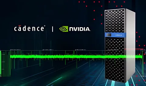
 Cadence has unveiled a major advance in pre-silicon power analysis, achieved in close collaboration with NVIDIA. By pairing the Palladium® Z3 Enterprise Emulation Platform with the new Dynamic Power Analysis (DPA) App, the companies have developed a method to analyse billion-gate AI and machine learning (ML) designs across billions of cycles in just a few hours, delivering accuracy levels of up to 97%.
Addressing the Scale Challenge
Today’s most advanced semiconductors demand vast computational resources to model accurately. Traditional power analysis tools often struggle to scale beyond a few hundred thousand cycles without requiring impractical timeframes. Cadence’s hardware-assisted acceleration and parallel processing innovations now enable performance verification on an entirely new scale, providing engineers with actionable insights at the earliest design stages.
According to Cadence corporate vice president and general manager Dhiraj Goswami, this breakthrough “redefined boundaries, processing billions of cycles in as few as two to three hours,” allowing teams to meet aggressive power and performance targets while accelerating time to silicon.
Precision Power Profiling
NVIDIA’s vice president of hardware engineering, Narendra Konda, emphasised the growing importance of efficiency in AI infrastructure, noting that the combination of Cadence’s EDA expertise and NVIDIA’s accelerated computing platforms “advances hardware-accelerated power profiling to enable more precise efficiency in accelerated computing platforms.”
By accurately estimating power consumption under real-world workloads, the DPA App enables engineers to validate functionality, power usage, and performance before tape out, when adjustments are still feasible. This is particularly valuable in AI, ML, and GPU-accelerated applications, where over- or under-design can lead to costly delays or inefficiencies.
Integrated for Efficiency
Palladium DPA is fully integrated into Cadence’s analysis and implementation environment, supporting power estimation, reduction, and signoff throughout the chip development process. This holistic approach helps deliver silicon and systems that meet performance targets while optimising for energy efficiency, an increasingly critical factor in competitive markets.
Learn more and read the original announcement here.


