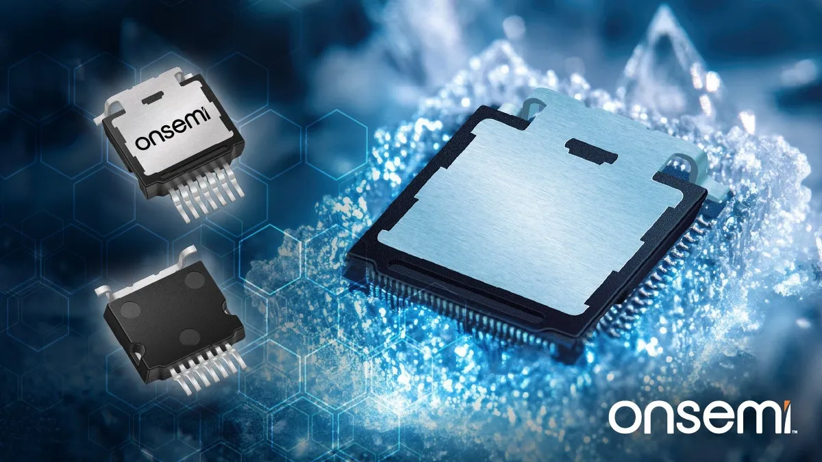
 As power systems push toward higher efficiency and greater output density, thermal constraints increasingly shape what engineers can achieve. Silicon carbide devices often deliver the switching performance required for fast, compact power stages, but the packaging around them can become a thermal bottleneck. onsemi has introduced a new approach by releasing its EliteSiC MOSFETs in the T2PAK top cool package, giving designers a way to move heat directly into the cooling structure rather than through the printed circuit board.
Why Top Cool Architecture Matters in High Power Platforms
Thermal management has become one of the defining challenges in applications such as EV traction inverters, solar inverters and energy storage systems. Higher switching speeds and rising power density push conventional surface mount packages toward their limits, especially when the PCB must serve as the primary thermal path. The T2PAK format changes this by relocating the heat extraction point to the top of the MOSFET, allowing the device to couple directly into a heatsink. For engineers, that allows thermal design to be driven by cooling hardware rather than copper area or heavy board layers, which opens space for more compact and efficient layouts.
A Packaging Model Designed Around SiC Performance
The EliteSiC portfolio is now available in both 650 V and 950 V variants using this top cooled architecture. The devices support a range of Rds(on) values from 12 mΩ to 60 mΩ, which gives engineers flexibility when balancing conduction loss, switching speed and thermal overhead. Because the T2PAK structure bypasses PCB thermal limitations, junction temperatures remain more stable under high loads and transient events. This reduces device stress and offers a path to longer operational lifetime in systems that face wide thermal swings, such as DC fast chargers or grid tied inverters. onsemi notes that the format maintains low stray inductance, which is important for switching performance and energy loss control at high frequencies.
Practical Integration Advantages for Automotive and Industrial Designs
The top cool configuration gives designers more freedom in mechanical layout. Instead of routing heat through copper planes and thermal vias, the MOSFET can attach directly to a system heatsink, simplifying the thermal path and reducing the number of compromises normally required in power stage design. The approach also combines benefits from both TO 247 and D2PAK packages without the drawbacks of large through hole footprints or thermally constrained surface mount formats. For engineers building compact inverter stages or power modules, this approach supports higher power density without aggressive PCB complexity or secondary thermal structures.
Implications for Next Generation Power Electronics
onsemi’s rollout of T2PAK devices signals a shift toward packaging innovations that complement intrinsic SiC advantages. With rising demand for efficiency and reliability across EV platforms, renewable infrastructure and industrial power systems, packaging can deliver competitive differentiation when device physics alone cannot meet thermal targets. By adopting a structure that channels heat directly into the cooling system, engineers gain margin that can be applied to switching improvements, smaller magnetics or tighter enclosures. For development teams working toward faster time to market, the simplified thermal strategy may also reduce mechanical iteration and validation cycles.
Learn more and read the original announcement at www.onsemi.com
You may also like