Applied Materials Advances GAA Transistor Engineering For Faster AI Chips At 2nm And Beyond
 As AI compute pushes deeper into the limits of what silicon can do, the performance of the transistor itself becomes the bottleneck rather than the architecture built on top of it. Many of the constraints now come from the interfaces between materials, the smoothness of nanosheets, or the resistance at the tiny contacts that link a device to its wiring layers. These are not problems that software or packaging can solve. They live at the atomic scale. Applied Materials is targeting that boundary with a set of systems designed to tune the physical structures that define Gate All Around transistors at 2nm and future angstrom nodes.
A shift toward GAA devices brings new challenges. Stacked nanosheets deliver better electrostatic control than FinFETs, but their performance depends heavily on how clean and uniform each sheet is. Small variations in surface roughness can slow carriers, weaken the channel or create inconsistencies that ripple through the entire device. As transistor dimensions shrink and sheet counts rise, traditional treatments struggle to maintain the level of precision needed for repeatable behavior. Applied’s approach tries to close that gap by engineering surfaces, trenches and contacts at a scale where small improvements change overall chip performance.
Radical Surface Treatment For Uniform Nanosheet Channels
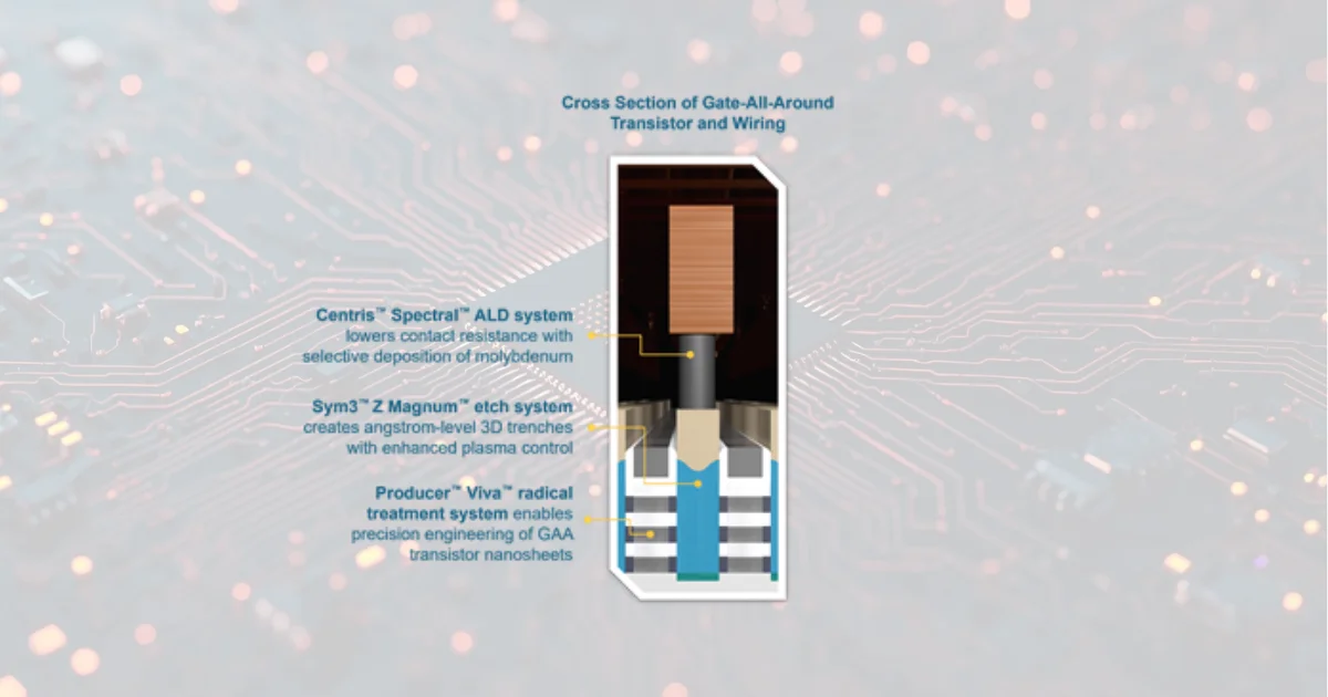
One detail worth noting is the Applied Producer™ Viva™ radical treatment system, which focuses on smoothing nanosheet surfaces with angstrom level precision. Instead of exposing the silicon to high energy ions that risk damaging the channel, the system generates ultra pure neutral radicals using a remote plasma architecture that filters out those charged particles. This lets the treatment reach buried structures without disrupting the thin sheets that carry current. A more uniform surface gives electrons a cleaner path, improving mobility and helping GAA devices switch faster at lower power. In practice, this addresses one of the subtle but persistent issues in nanosheet fabrication, where even slight contamination or roughness becomes a performance limiter.
Etch Control That Defines High Aspect Ratio 3D Structures
Another constraint in GAA manufacturing is the etching of deep, narrow trenches that house the stacked nanosheets. These trenches need extremely straight sidewalls and precise bottom shapes to ensure consistent device geometry. Applied's Centris™ Sym3™ Z Magnum™ etch system brings a new generation of pulsed voltage technology that independently tunes ion direction and ion energy. This allows the tool to target the wafer with defined ion trajectories rather than relying on broad plasma behavior. When working at angstrom scale dimensions, this level of control determines whether nanosheets emerge uniform enough to sustain high switching speeds. The approach also benefits DRAM and HBM designs, where taller stacks and denser arrays depend on consistent trench profiles.
Molybdenum Contact Formation To Reduce Resistance
As devices scale below 2nm, contact resistance becomes a larger share of total device resistance. Tungsten has been the industry’s default material for years, but its limits are becoming more visible at the smallest geometries. The Applied Centris Spectral Molybdenum ALD system introduces selective deposition of monocrystalline molybdenum as a lower resistance alternative. Molybdenum can be deposited thinner without degrading conductivity, which helps reduce the bottleneck where transistors hand off current to the interconnect network. Small reductions in contact resistance make a measurable difference in AI workloads, where billions of switching events amplify every inefficiency. This step also helps maintain energy efficiency as wiring stacks get more complex.
Contributions To Angstrom Era Scaling
These systems arrive as foundries begin ramping 2nm class processes into production. The combined effect of better nanosheet surfaces, cleaner trenches and lower resistance contacts helps unlock more of the theoretical performance gains promised by GAA architectures. Without these improvements, the benefits of switching to nanosheets would be constrained by the imperfections introduced earlier in fabrication. Applied positions the new tools as extensions of its long standing role in major transistor inflections, suggesting they will support both current nodes and the first angstrom class processes that follow.
Impact On AI Compute Roadmaps
AI acceleration depends on switching speed, power efficiency and wiring performance as much as it depends on architecture. Improvements at the atomic scale translate into lower voltage operation, faster transitions and better thermal behavior. These advantages accumulate across billions of transistors. As AI chips become increasingly limited by physical constraints rather than core count, the kind of materials engineering described here plays a growing role in determining how far compute performance can scale each generation. With multiple leading logic manufacturers already deploying these systems, the work at this level of the stack quietly shapes the capabilities of future AI hardware.
Learn more and read the original announcement at www.appliedmaterials.com
You may also like