 Recently, researchers have developed a new memory chip that supposed breaks the rules of miniaturization, helping to solve the issues faced with overheating. What challenges does reducing memory technologies introduce, what did the researchers develop, and how could it help with the future of electronics?
What Challenges Does Shrinking Memory Technologies Face?
Memory comes in a wide range of different types, all of which has have their own pros and cons. For example FLASH is great for long-term storage but faces limitations on its max write cycles, while SRAM provides high-speed access, but is costly to implement. Because of the many limitations faced, most designs will utilise a mixture of technologies to create a complete system.
To improve these technologies, engineers will do all they can to reduce the size of each memory technology as much as possible, so as to maximise memory density. However, any engineer who wants to reduce the size of any re-programmable memory technology will immediately face numerous problems.
In almost every case, the ability to store information comes from being able to control an electric charge, whether it’s the voltage across a capacitor (such as in DRAM), or the ability to trap electric charge in a floating gate (such as FLASH). When trying to reduce the size of a memory cell, the amount of charge that it can hold will also reduce, meaning that such cells will be more susceptible to noise. Furthermore, reducing the size of components also increases the chances of leakage, making it hard to retain information.
Finally, when reducing the size of memory to extremely small sizes, the amount of heat generated also increases, making it hard to store charge reliably. This is why DRAM requires frequent refresh cycles, and why FLASH memory needs to take great care when trying to trap charges.
Regardless of the memory technology, trying to make it smaller presents engineers with a whole host of challenges, which is why it is not commonly done. However, a group of researchers has recently proven that memory technologies can be made significantly smaller than currently thought.
Researchers Develop New Memory Technology
Recently, a team of researchers from the Institute of Science Tokyo announced the development of a new nanoscale memory device that, instead of degrading as it shrinks, actually becomes more efficient. The research builds on top of another memory technology called “Ferroelectric Tunnel Junction” (FTJ) memory that stores information by using an electric polarisation to switch the current flowing through a barrier.
While FTJs have shown some promise, they suffer from the same issues faced by other technologies; shrinking results in degradation. One area that this occurs in particular is the need for very thick barriers between two electrodes, as this helps to minimise leakage. However, as the barrier becomes thicker, it becomes more resistive, thereby reducing the number of bits that can be stored.
So in light of these challenges the team at the Institute of Science Tokyo decided to approach this problem differently to previous attempts. Instead of trying to find materials that would express polarisation at smaller sizes, they turned their attention to the issue with leakage current.
In order for a FTJ to function, both electrodes need to be connected to a polarised material (such as a ferroelectric), but in standard implementations, these two electrodes are formed as simple plates over the top of the ferroelectric material. But as these electrodes touch at their sides, small boundaries between the two form, and this boundary often creates crystal imperfections, resulting in electrical leakage.
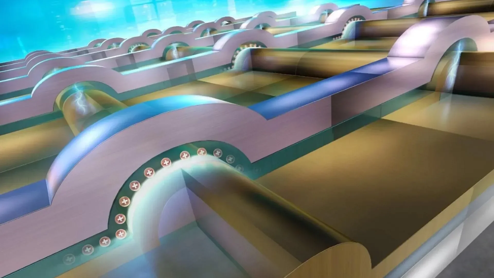
To overcome this, the team reduced the overall size of the FTJ memory cell to just 25nm in width, using a 12nm-thick hafnium oxide barrier and 15nm electrodes. By shrinking the device and redesigning the structure to minimize the number of crystal boundaries, specifically by forming semicircular electrodes that help create a near single-crystal structure, they significantly reduced energy loss from leakage and minimized heating effects, which are major challenges in conventional semiconductor devices.
This approach challenges conventional expectations by improving memory performance as the device shrinks, rather than degrading it. Such technology could enable ultra-efficient electronics, including longer-lasting mobile devices, low-power IoT systems, and more energy-efficient AI hardware.
Additionally, because the fabrication method is compatible with existing semiconductor manufacturing processes, it holds promise for easier industry adoption.
Could this New Technology be the Future of Electronics?
The use of single-crystal designs and the minimising of boundaries is certainly impressive, and it also makes perfect sense when considering the advantages brought by single-crystal semiconductors. Furthermore, what the researchers have demonstrated here is nothing short of genius; taking a technology and making it better as it shrinks.
Of course, this doesn’t mean that the technology is ready for mainstream use, as the device was demonstrated in a laboratory with no practical application. Thus, the next step for the researchers is to try and scale up the design to see how it performs in a real-world scenario.
Scaling up any technology presents all kinds of new challenges. It is not yet clear whether the benefits observed at the nanoscale can be preserved when producing larger chips with billions of memory cells, as required for commercial products.
The researchers will need to develop methods to fabricate these structures reliably at scale, ensuring consistent performance, durability, and integration with other circuit elements. If they succeed, this memory could become an important contender for future electronics.
Lower energy and higher density memory is especially valuable for applications such as AI and IoT, which are increasingly limited by power consumption and memory bandwidth. If this technology can be produced with existing manufacturing infrastructure, it could accelerate the development of more efficient, advanced computing systems in the years to come.
You may also like