
 Researchers recently found a solution to get even smaller monolayer structures to function as transistors more effectively, paving the way to a future beyond 0.42nm. What did the researchers do and could the future of semiconductors lie in monolayers?
Researchers Develop 0.42nm Technology
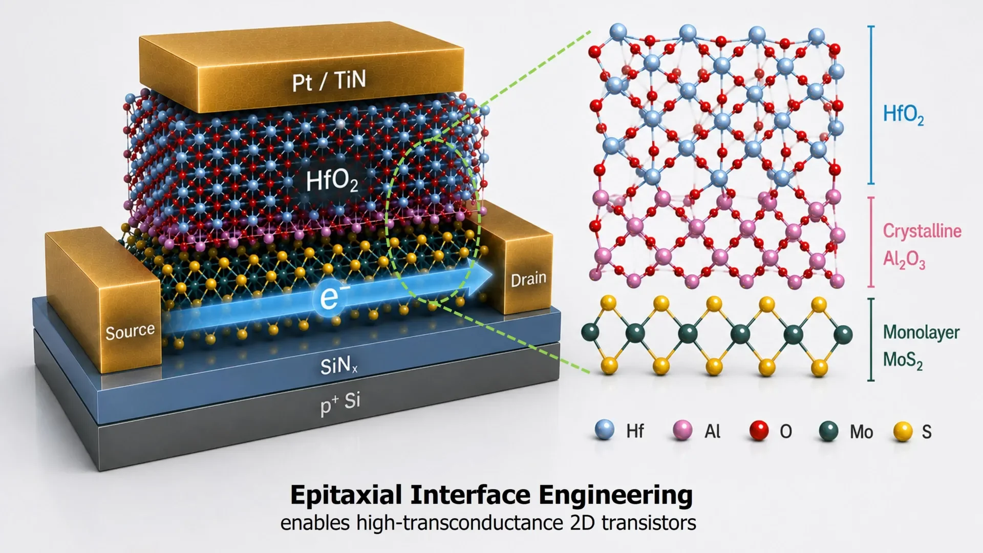
Recently, researchers from National Yang Ming Chiao Tung University (NYCU) and TSMC Corporate Research developed an interface-engineering technique that could help improve the performance of atomically thin transistors. While such thin semiconductor films have been explored for decades, one of the major challenges faced is the need for an extremely thin gate dielectric, which sits between the semiconductor channel and the gate.
If not done carefully, adding a dielectric layer can disrupt the semiconductor-dielectric interface, resulting in a reduction in electron mobility and therefore impacting transistor performance. In order to solve this issue, the team engineered the interface by placing an ultrathin epitaxial aluminium layer on top of a monolayer of molybdenum disulfide (MoS₂).
This aluminium layer was then oxidised to form a roughly 0.42 nm aluminium oxide buffer, followed by the addition of a high-κ hafnium oxide gate dielectric. The resulting atomic-scale buffer creates a smoother surface for the dielectric to grow on, while also limiting unwanted electrical interactions between the materials.
This allows the transistor to maintain strong gate control without sacrificing carrier transport, addressing one of the major trade-offs involved in creating extremely small transistors.
The latest findings were demonstrated using CVD-grown monolayer MoS₂ in a back-gated transistor setup. The resulting devices achieved an equivalent oxide thickness of approximately 1 nm, while also demonstrating low leakage and minimal hysteresis.
Furthermore, the devices achieved a maximum transconductance of 0.45 mS μm⁻¹ with channel lengths of approximately 100 nm. This demonstrates that thin dielectric scaling, strong electrostatic control, and high carrier mobility can be achieved simultaneously in a 2D transistor.
Another important aspect of the research is that the team used CVD-grown MoS₂ rather than laboratory-exfoliated flakes. This is significant because CVD is more compatible with wafer-scale manufacturing, which will be essential if these materials are ever to move beyond laboratory demonstrations and into commercial semiconductor production.
Of course, further optimisation will still be required before this technology can be considered ready for commercial use. However, the results suggest that as transistors approach atomic dimensions, engineering the interface between materials could become just as important as developing new semiconductor materials.
If this approach can be developed further, it could eventually support low-power 2D electronics that operate at dimensions beyond what is practical with conventional silicon-based transistor structures.
Could the Future be in Monolayers?
As researchers continue to shrink the size of transistors, the use of atomic structures will inevitably put a limitation on what can be done. Eventually, conventional three-dimensional crystalline structures become increasingly difficult to interface with when creating transistors at atomic scales.
But there exists another type of structure; those that are only one atomic layer in height.
Just like how crystals can be used to make semiconductors, monolayers are also specific structures that have a very defined shape and behaviour. Furthermore, considering that these layers are incredibly thin, if switching devices can be made using them, then the active semiconductor structure is already approaching the smallest dimensions physically possible.
This is why researchers are actively looking at monolayers to see if they can be used in commercial semiconductor devices. Instead of simply continuing to shrink conventional silicon structures, 2D materials provide researchers with a completely different approach to semiconductor scaling.
The recent work from researchers in Taiwan demonstrates that some of the challenges involved in making these devices function can be addressed through careful engineering of the interfaces between materials. Rather than the semiconductor itself being the only consideration, the way that the gate dielectric interacts with the atomically thin channel becomes equally important.
Of course, these devices haven't been commercialised just yet, and there are still significant challenges involved in manufacturing, optimisation, and integrating 2D materials into practical semiconductor processes.
However, considering that planar devices can be made by growing layers at specific atomic heights, it is increasingly possible to imagine a future where semiconductor devices are built from structures only a few atoms thick.
If researchers can solve the remaining manufacturing challenges, monolayers could eventually become an important part of the future of semiconductor technology.
Now, the race is on to see who can produce the first functional commercial devices, and how quickly researchers can get them from the laboratory and into real-world applications.
You may also like