 Just when you thought they couldn’t make them smaller, researchers from IBM have just demonstrated a new chip using a new nanostack design, supporting over 100 billion transistors on a single chip. What did IBM demonstrate and how could this help shape future devices?
IBM Demonstrates New 0.7nm Chip
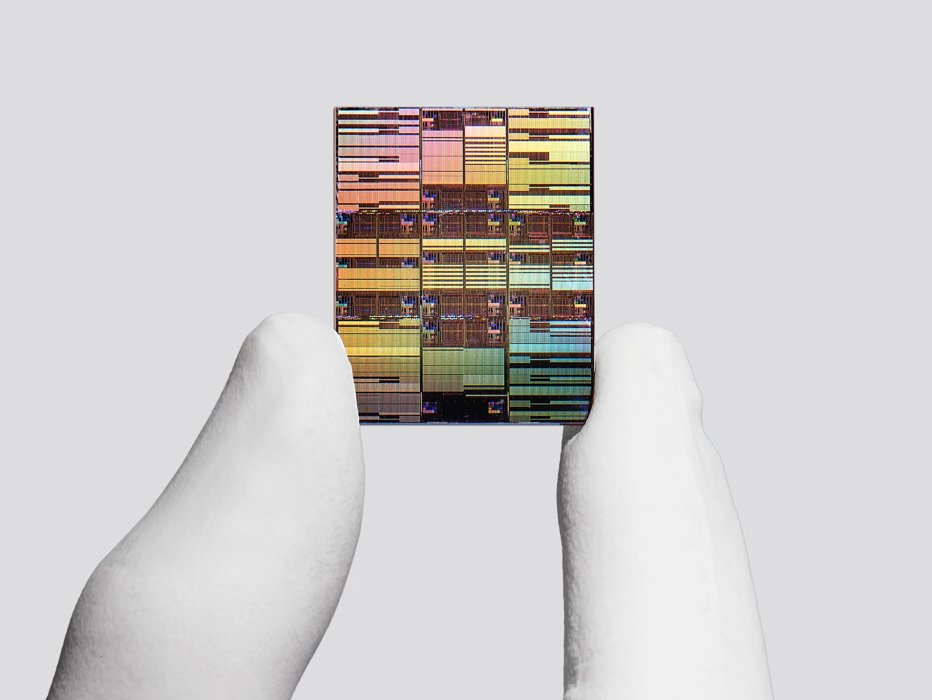
Recently, IBM announced that they have managed to integrate 100 billion transistors onto a single chip using a new 0.7nm process, something that has surprised many.
This latest semiconductor development is based on what IBM describes as a “nanostack” architecture, which combines stacked nanosheet transistors in a vertical arrangement rather than relying solely on horizontal scaling. The idea is not simply to shrink individual features further, but to build upward, stacking functional transistor layers in a controlled 3D structure.
In this design, nanosheets are arranged in multiple vertical layers, with each transistor gate electrically isolated and independently controlled. This separation allows engineers to optimise each layer using different materials or geometries, depending on its role in the overall structure. In practice, this means performance and efficiency can be tuned more precisely than in traditional planar or even single-layer nanosheet designs.
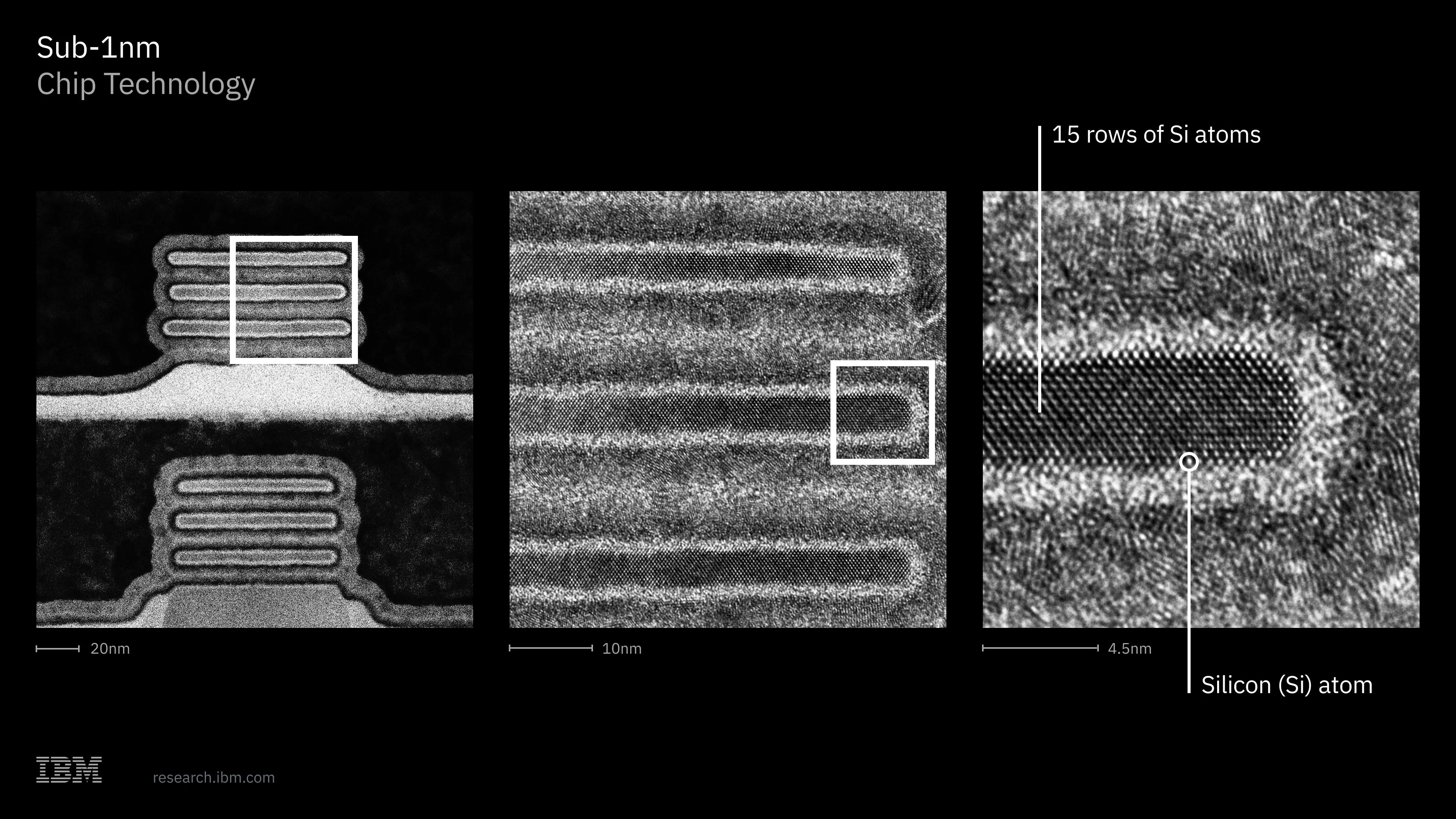
IBM has said that this approach enables extremely high transistor density as demonstrated with 100 billion transistors integrated into a single die roughly the size of a fingernail. This corresponds to a density on the order of around a billion transistors per square millimetre, depending on how the effective area is calculated across stacked layers.
Now the significance here is not just density of devices, but the method used to achieve it. Instead of continuing to push lithography into increasingly extreme resolution limits, the nanostack approach redefines scaling as a three-dimensional engineering problem.
IBM also states that, compared to its previous 2 nm-class technology, the new architecture could deliver up to 50% higher performance or up to 70% better energy efficiency, depending on workload and configuration. Additional improvements in SRAM scaling of around 40% have also been stated, which is critically as on-chip memory often becomes a limiting factor in modern processor design.
But it is also important to note that this remains a proof-of-concept demonstration. The chip certainly validates that the architecture can operate as functional CMOS circuitry, but it is by no means yet a commercially deployed manufacturing process.
How Could this Help Shape Future Devices?
The most immediate implication of IBM’s work, interestingly, has nothing to do with the headline transistor count, but instead what that density enables at a system level.
More transistors allow for larger CPU clusters, more GPU cores, additional hardware accelerators, and significantly expanded cache and on-chip memory structures. In practical terms, what this really means is that it has the ability to reduce the need to move data off-chip, which is often one of the largest sources of both latency and power consumption in modern computing systems.
Another major implication of this technology is the introduction of stacked nanosheet structures, pointing towards a longer-term transition where semiconductor scaling is no longer defined purely by shrinking feature sizes on a flat plane. Instead, this use of vertical integration begins to resemble a volumetric design problem, where performance gains come from adding functional layers vertically.
This is important because traditional scaling approaches are increasingly constrained, where improvements in lithography alone are becoming far too difficult and expensive to achieve. Considering that only one company in the world are capable of creating such image patterners (ASML), it becomes obvious why engineers are going down the 3D stacking route.
If this direction continues, future chips may increasingly rely on stacked logic, stacked cache, and even stacked memory regions integrated directly into compute layers. Such designs could enable higher core counts, larger local memory pools, and more specialised accelerators dedicated to specific workloads, all within a single package.
This stacking approach also aligns with existing trends in advanced packaging, where multi-die stacking is already being used in high-performance processors. The difference here, however, is that stacking moves from the package level down into the transistor architecture itself.
Of course, this remains early-stage research, and many of the claimed benefits depend on manufacturing maturity, yield, and thermal management at scale. But the key point is that the direction of travel is now clearer. Rather than relying solely on ever-smaller features, the industry is beginning to treat transistor density as something that can be built vertically as well as laterally.
You may also like