
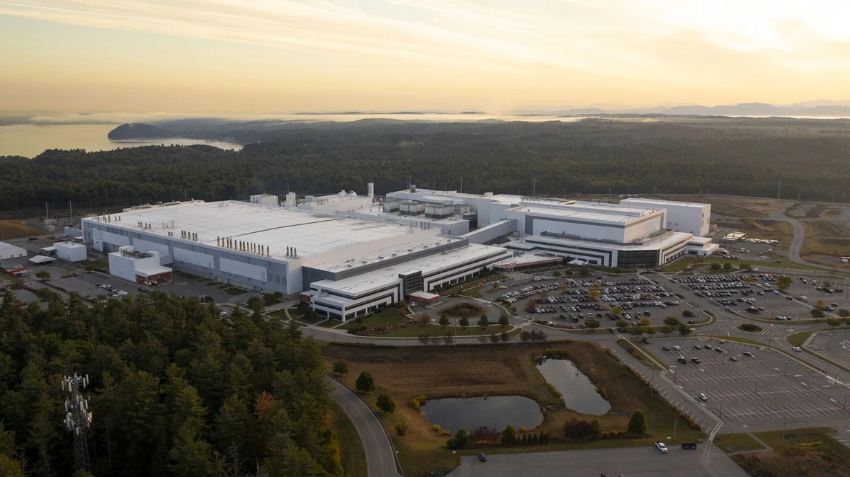
 GlobalFoundries has made the process design kits for two new CMOS technologies available to chip designers. On the face of it, the launch of a 40 nm and 22 nm semiconductor process might seem fairly removed from the enormous amount of attention currently surrounding artificial intelligence. Look at what those processes have been designed to do, however, and the connection becomes much more interesting.
The new 40UX and 22UX platforms target devices combining processing with sensing, analogue electronics and connectivity. GlobalFoundries sees applications ranging from low-power MCUs and wireless devices through to imaging systems, mixed-signal SoCs and edge AI. This is a very different picture of AI hardware from the GPUs, accelerators and high-bandwidth memory dominating discussions around the data centre.
If intelligence is going to move into cameras, sensors, industrial equipment, wearables and other connected devices, the semiconductor requirements change with it.
The Cloud Can't Do Everything
Most of today's largest AI systems depend on enormous amounts of computing infrastructure. Data centres can dedicate racks of accelerators, large quantities of memory and substantial amounts of power to training and running models. An edge device has none of those luxuries.
A wireless sensor might spend much of its life running from a battery. A camera needs to capture and process information while operating within a relatively small thermal envelope. An industrial controller may need deterministic communication with other equipment while simultaneously handling sensor inputs and local processing. These are very different environments, and sending everything back to the cloud isn't always practical.
Network latency matters in systems that need to respond quickly, while reliable connectivity isn't guaranteed everywhere. Transmitting data also consumes power, and some information may be better kept locally for privacy or security reasons. None of this means every edge device suddenly needs a powerful AI accelerator. In many cases, the amount of local intelligence required may be relatively modest.
What these devices do need is an efficient way of combining processing with everything else required to interact with the physical world. That starts to change what engineers need from the underlying semiconductor technology.
40 nm Isn't Suddenly Old Technology
Discussion around semiconductor manufacturing tends to focus heavily on the smallest available process node. The industry moves from 7 nm to 5 nm, then 3 nm and beyond, and it can be tempting to assume that anything manufactured on a considerably larger node has simply been left behind. For many embedded applications, that isn't particularly useful.
GlobalFoundries' 40UX platform is based on the company's existing high-volume 40 nm technology. Rather than chasing maximum transistor density, it combines ultra-low-leakage transistors and SRAM with embedded flash, low-noise analogue capabilities and RF support.
Those characteristics make more sense when considered against the devices GF is targeting. A Bluetooth Low Energy MCU doesn't simply need processing performance. It needs memory, wireless connectivity and potentially analogue interfaces while consuming very little power, particularly when the device spends long periods waiting for something to happen. Embedded non-volatile memory can also be useful in these systems, and 40UX includes high-endurance embedded flash as part of the platform.
It's a reminder that process-node choice is about much more than transistor size. For an edge device, the most appropriate semiconductor process may be the one that provides the right combination of digital logic, memory, analogue, RF, leakage, reliability and cost.
GlobalFoundries plans to ramp 40UX into volume production at its Singapore facility in 2027, with production in Malta, New York planned later. Automotive Grade 1 qualification, high-voltage and noise capabilities and enhanced embedded non-volatile memory are also on the roadmap.
AI at the Edge Still Has to Interact With the Real World
The 22UX platform approaches the problem from another direction. Built around a 22 nm process, it is aimed at applications requiring greater analogue integration and sensing performance, including imaging, mixed-signal systems and edge AI.
That analogue element can easily get lost when talking about artificial intelligence. A model running in a data centre is already working with digital information, whereas a physical device may first have to measure temperature, detect movement, capture an image, listen to audio or interpret another signal from its environment. Before any intelligent processing can happen, the electronics need to acquire that information accurately.
GF has therefore put considerable emphasis on analogue performance with 22UX. The platform includes low-noise analogue devices, improved device matching and wafer-scale Random Telegraph Signal noise characterisation. It also supports low-noise 3.3 V analogue FETs and is being positioned for applications including stacked CMOS image sensor readout ICs.
Bonding-ready wafers provide another indication of where these systems may be heading. Rather than placing every function onto one monolithic piece of silicon, advanced packaging and 3D integration can bring different technologies together more closely. A sensing layer, for example, could be paired with processing electronics designed specifically to handle the resulting data. For edge AI systems where sensing and processing increasingly need to operate together, that relationship becomes particularly interesting.
Could Compute Move Into the Memory?
One of the more interesting items on the 22UX roadmap is analogue compute-in-memory. It isn't part of the platform available today, and GlobalFoundries hasn't provided detailed implementation information in this announcement, but its inclusion points towards another problem engineers are trying to solve as AI processing moves into power-constrained devices.
Computation itself isn't the only thing consuming energy. Moving data between memory and processing hardware also has a cost, particularly for AI workloads that can involve repeatedly transferring large quantities of model data between memory and compute resources.
Compute-in-memory architectures attempt to reduce some of that movement by performing certain operations closer to, or within, the memory where the data is stored. Whether analogue compute-in-memory ultimately becomes a major part of mainstream edge devices remains to be seen, but its appearance alongside embedded memory, low-leakage devices and analogue optimisation shows how differently the edge AI problem can be approached compared with simply adding more processing cores.
AI Hardware Won't All Look Like a GPU
There is inevitably plenty of AI terminology surrounding GlobalFoundries' announcement. The company describes the UX family as part of its technology portfolio for "Physical AI", a phrase appearing increasingly often across the electronics industry. Underneath that language, however, is a fairly practical engineering problem.
If more processing moves into the devices collecting information from the physical world, those devices still need to sense, communicate, store data and control whatever they're connected to. That requires a different balance of semiconductor technologies.
At one end of the AI industry, data centres are moving towards enormous amounts of specialised compute, high-bandwidth memory and increasingly powerful accelerators. At the other, engineers may be trying to perform a relatively small amount of useful local processing within a sensor, wireless MCU, camera or industrial device that has a fraction of the available power.
GlobalFoundries' 40UX and 22UX platforms illustrate some of the technology that could sit underneath those systems: low-leakage logic, embedded memory, analogue electronics, RF connectivity, sensing support and potentially new ways of bringing memory and compute closer together.
The future of AI hardware therefore isn't necessarily a race towards one type of processor or one manufacturing node. If intelligence really does spread into billions of physical devices, some of the most important semiconductor technologies enabling it may look very different from the chips currently filling AI data centres.
You may also like