 As researchers approach the fundamental limits of transistor design, some are now looking to go up rather than down. What challenges does chip stacking face, what have researchers recently demonstrated, and why is this the future of semiconductor technologies?
What Challenges Does Chip Stacking Face?
Over the years, the semiconductor industry has been able to continually make chips smaller, faster, and cheaper. However, this shrinking trend is now starting to slow down, and it won’t be long before transistors reach their physical limits. When this happens, there will no longer be any increase in computational power simply by making transistors smaller.
Thus, researchers are being forced to explore other options such as going up, whereby multiple active semiconductor layers are stacked on top of each other to increase transistor densities. But while researchers continue to develop new techniques for achieving chip stacking, there are numerous challenges faced with chip stacking, even when using traditional 3D structures.
To start, chips have always been designed on flat semiconductor wafers with a single semiconductor layer. But if additional layers are being stacked, then these active layers must be either grown on top, or worse, involve multiple layers physically stacked on top of each other which introduces massive challenges with alignment.
Another challenge faced is the need for inter-posers and interconnects. Stacking dies and exposing contact points for dies to make contact is much easier said than done. Everything from bonding methods to alignment and signal integrity all cause issues, which is why die-to-die bonding has only seen recent adoption by bleeding-edge technologies.
Finally, the characteristics of grown active layers on top of dies would likely be extremely poor. This primarily comes down to the fact that there wouldn’t be substantial semiconductor wells between the active layers, meaning that signals may bleed into adjacent layers. Worse, if an active layer doesn’t have enough semiconductor well below it, then the resulting thermal characteristics can suffer enough that it becomes impossible to keep cool.
Researchers Create Three-layer Active Semiconductor
Recognizing the challenges faced with Moore’s Law, the semiconductor industry is actively trying to find new solutions. One solution that has shown promise is chip stacking, whereby multiple active dies are combined onto a single package, but even then, challenges still exist.
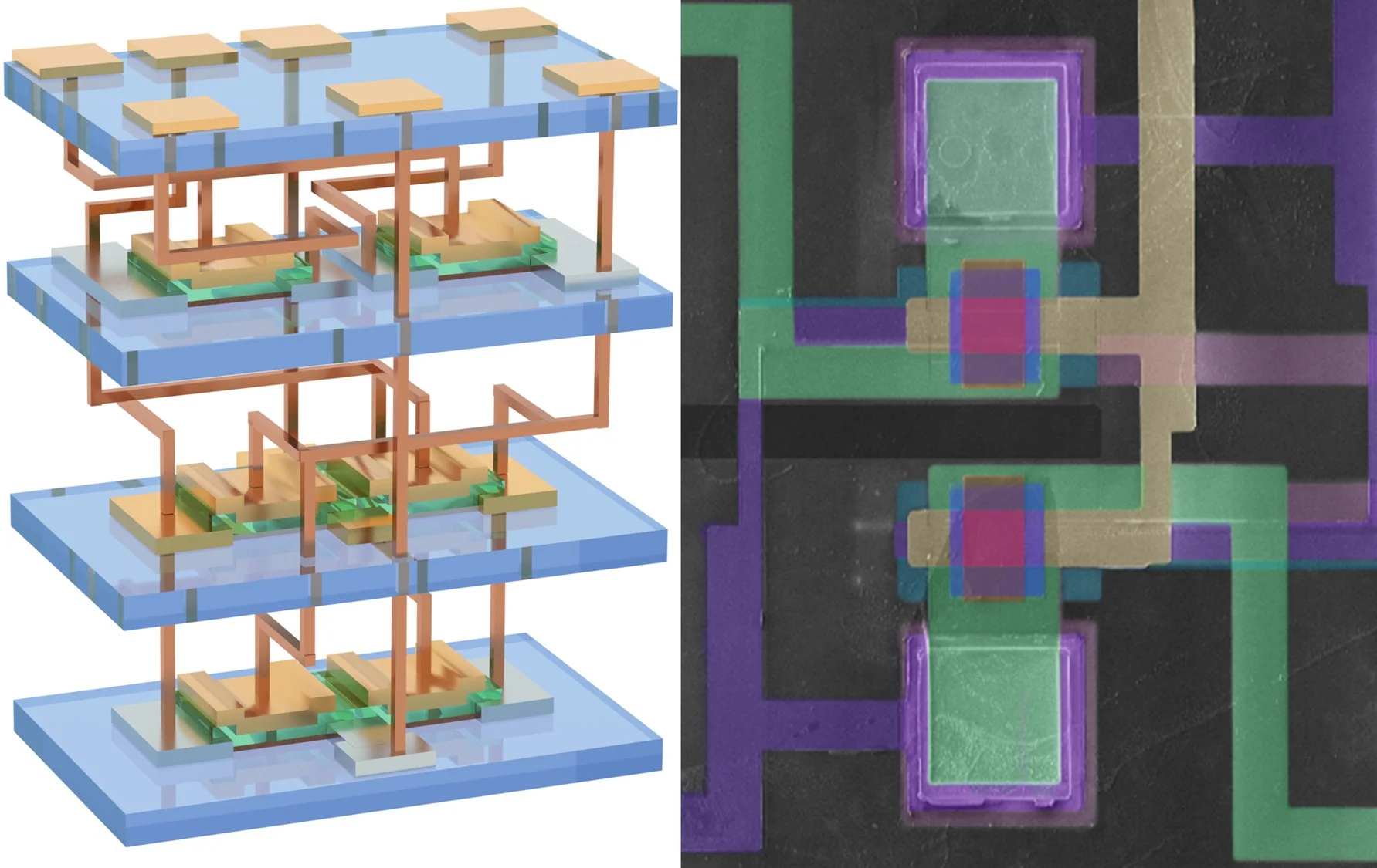
Recently, a team of researchers from the University of Illinois Grainger College of Engineering have been working on a new technique that could very well become the key technology for future devices. Instead of trying to place transistors side by side, the researchers instead turned to the vertical, with a 3D monolithic chip integrating active silicon layers directly on top of each other.
While not the first to do so, the researchers were able to take their technique further by combining multiple active layers that were directly built on top of each other. Currently, there are numerous methods for combining different chip layers (such as high-bandwidth memory and 3D V-Cache), but these are limited to dies stacked on top of each other. Furthermore, these designs are reliant on through-silicon vias and the ability to precisely align dies together.
However, the team at University of Illinois Urbana-Champaign went one step further by combining three separate layers. To achieve this, the researchers took advantage of ultrathin single-crystalline silicon nanomembranes that were transferred at low temperatures (less than 200 degrees Celsius). At the same time, the researchers also adopted junctionless transistor designs and heavily pre-doped channels to eliminate the need for high-temperature doping steps during fabrication, thereby allowing the team to retain the thermal budget limitations of typical 2D chips.
The result of the researchers' work was the creation of three stacked silicon layers that could each operate independently while simultaneously operating as a single functional unit. The team also noted that their approach allows for 3D logic elements and SRAM designs, and is now looking to move their process forward with the intention of working with semiconductor foundries, including IBM, Intel, and TSMC.
Why the Future of Semiconductors is Up
For anyone who follows my work on The Component Club, you’ll know that I often say the same thing whenever new chip stacking techniques are announced, “the only logical option is to add more active layers”. And it’s true, out of all the techniques being developed, adding more active layers makes the most sense.
To start, engineers can spend less time trying to make things smaller, and instead turn their focus to trying to solve problems such as alignment and crystal deposition. Once this problem is cracked, it only makes sense that adding additional layers becomes a more trivial problem.
With such a capability, devices will rapidly increase in device density, helping with memory densities, processor core counts, and much more. In fact, it is even possible that devices could go back on node size, utilising older nodes, which helps with the production process (as it eliminates the need for bleeding edge technologies such as EUV).
Finally, stacked designs have major benefits, such as decreased distance between circuits and modules, reducing signal latency, and memory near processing systems. Even the addition of one extra active layer can immediately double the number of transistors on a design. There are numerous other advantages to stacked designs, including the ability to reuse older semiconductor nodes, but overall, there is no doubt that going up is the only viable option for the future.
You may also like