 The number of transistors on individual devices always seems to grow, and TSMC is now looking to shortly break the one trillion transistor mark, integrating an unbelievable number of devices on a single chip. What has TSMC announced, why do we face challenges when shrinking transistors, and where could this lead?
TSMC Marks One Trillion Transistor Milestone
Recently, TSMC announced that at their recent 2026 Europe Technology Symposium, that they are working towards having one trillion transistors per package by 2030. The addition of advanced packaging and new process nodes will not only enable next-generation semiconductors, but help to continue the development of key technologies such as AI.
According to TSMC, achieving such goals will come from not just the use of new nodes and smaller transistors, but the use of advanced packaging techniques such as CoWoS and SoIC. The new silicon node strategy by TSMC is expected to include A14 in 2024, N2P in 2026, N2U in 2028, and A13/A12 in 2029.
The A13 and A12 will offer optical shrinking to improve performance, while the N2P will provide transistor density improvements through the use of N2U derivatives. The combination of these different nodes will also see major improvements to energy efficiency, with TSMC expecting to improve energy efficiency by 30% by 2030 compared to 2024.
But, TSMC also noted that transistor reductions alone will not be enough to see continued improvements, and this has been hinted at for years by other semiconductor manufacturers who are now turning towards alternative measures. TSMC specifically mentioned that they expect to see ~30% more power reduction per node going forward, but this will come from increased R&D efforts in transistor design itself (such as CFET).
What Challenges Do We Face When Shrinking Transistors?
While the idea of a trillion transistors on a single chip may seem like a lot, when considering that modern processors have north of 100bn transistors, it becomes apparent that a trillion transistors is going to happen soon. Interestingly, this raises the question on whether transistor reduction provides the same benefits it once did.
As was previously mentioned, the cost of producing new devices is now becoming far too expensive, and the rate of technological advancement from simply reducing the size of transistors isn’t providing the same returns that it used to.
This can be seen when looking at what TSMC has been actively developing over the past few years. To start, TSMC is actively working on stacked technologies, which will likely be based on 3D NAND-like technologies, where additional active layers are added to a die as epitaxial layers. This enables more transistors to be integrated into a single package without needing to reduce the size of each transistor.
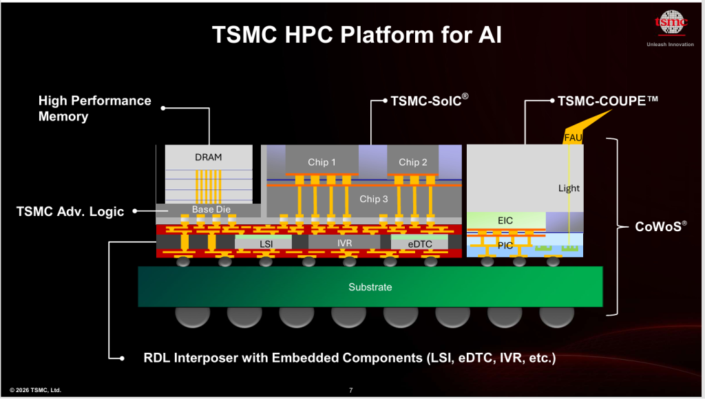
The second technology that TSMC is actively developing is advanced packaging. Such technologies allow dies to be combined, and the use of dies instead of monolithic designs reduces the total number of transistors needed on each layer, thereby improving yields.
Finally, TSMC is looking at technologies such as COUPE, which combine optics and ICs to create high-performance systems. Thus, large optical arrays can be mounted onto a package alongside an IC, and the combination of the two enables the creation of very powerful optical accelerators.
All of these technologies present numerous opportunities to engineers, especially those involved with AI and other computation heavy applications. But why are these technologies better than simply reducing transistor sizes? What challenges do engineers face when shrinking transistors?
By far, the biggest challenge faced is when we reach atomic scales. At this scale, transistor feature sizes becomes smaller than 1nm, and when this happens, numerous physical effects take place, ranging from quantum effects like electron tunneling to serious issues with heat dissipation.
Manufacturing at this scale also introduces technical hurdles, with one being involved with using light to image features that is orders of magnitude smaller than the wavelength of the incident photons used to create the exposure. Using extremely short wavelength UV to try and solve this challenge can cause significant damage to the underlying silicon, resulting in failed devices.
Another challenge faced is the electrical characteristics of nanometre-scale devices. As transistors approach the angstrom scale, electrons begin to exhibit more than just quantum behavior, other effects such as shot noise and random fluctuations in electron travel times also become critical.
Such effects can significantly impact the performance and reliability of nanometer-scale transistors, leading to reduced switching speeds, increased power consumption, and increased variability between devices. These effects can be difficult to model and predict, requiring extensive simulations and testing to optimize transistor design and fabrication processes.
Where Could this Lead Us?
Looking at what TSMC is doing, it seems more likely that we will start to move away from reducing transistor size, and instead, look towards stacking technologies. While such technologies are still in their infancy, there is no doubt that they will become dominant over the next decade, providing engineers with the ability to massively increase the number of transistors on any given die.
Additionally, the use of stacked dies will also help with increasing transistor count, as the combination of dies allows for reducing the total number of transistors on any one die, thereby increasing yields. Finally, the use of stacked dies also allows for mixing and matching of different functions, such as a memory chip directly connected to a processor.
For example, a SoM could be designed to integrate multiple memory chips onto a single package, and then combine this with an ASIC or processor. From there, AI accelerators can be used to offload AI tasks from the main processor, while high-speed data buses can provide low-latency connections between various dies, thereby increasing overall system performance.
Overall, it is clear that the semiconductor industry is starting to move away from the idea of reducing transistor size, and this will likely be beneficial in the long run. As we move towards 3D designs, it is possible that we will see significantly improved processing powers, which will not only help to solve the energy crisis, but also accelerate technological developments.
You may also like