
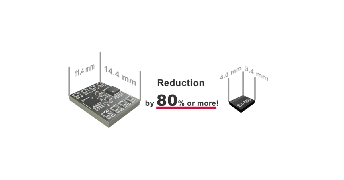
 Nisshinbo Micro Devices has developed a 3D mounting technology called Silicon Motherboard (Si-MB), which forms circuits on both sides of a silicon substrate and integrates ICs and passive components into a single package. In a window comparator prototype, the company reduced the mounting footprint by about 80% compared with a conventional discrete configuration.
The technology combines functional ICs mounted on the top surface of the silicon substrate with components formed inside the substrate using wafer processing. External passive components can then be mounted on the underside.
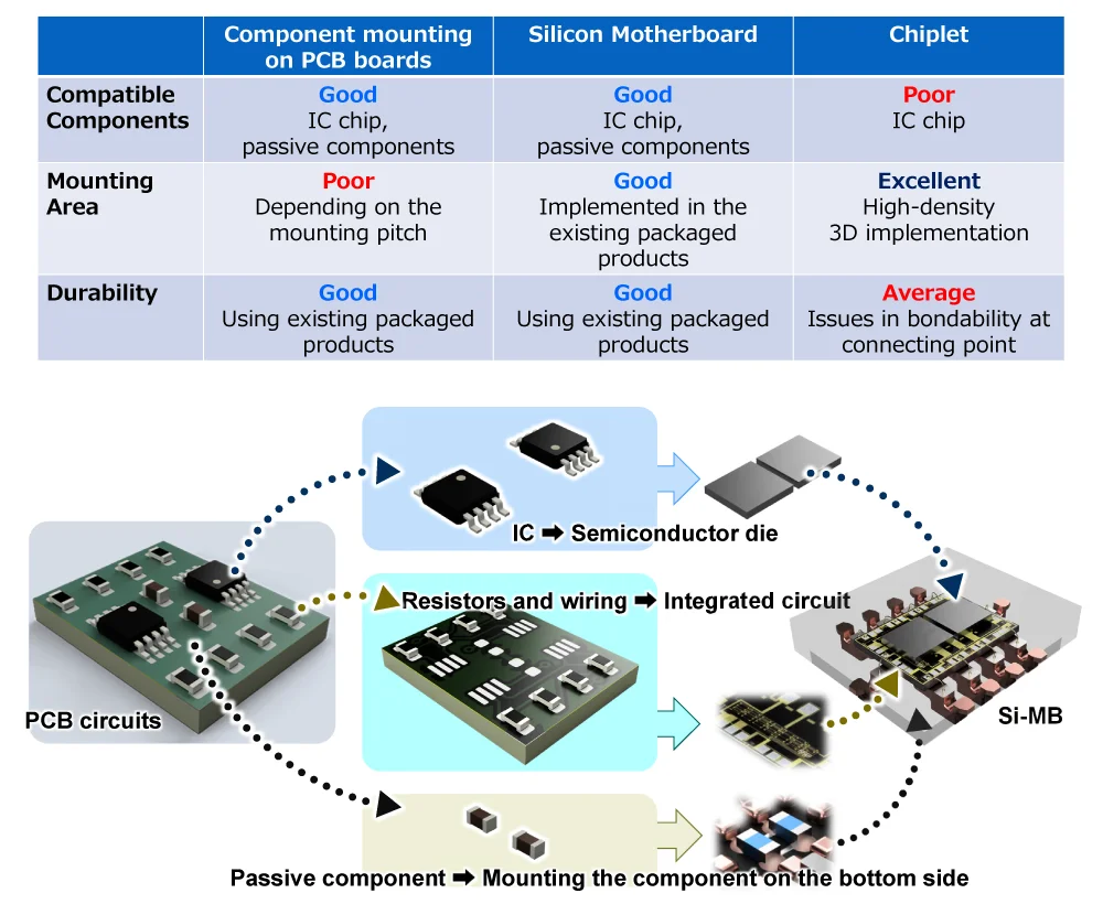 Figure 1: Issues of chiplet technology and overview of Silicon Motherboard
Nisshinbo describes Si-MB as the world's first 3D mounting technology of this type, based on its own research.
Passive Components Added to Silicon Integration
A key part of the Silicon Motherboard structure is the ability to mount external components on the bottom of the silicon substrate. Nisshinbo says this makes it possible to incorporate passive components that are difficult to integrate using conventional chiplet approaches, including capacitors above 1,000 pF, resistors below 1 Ω and inductors.
Transistors, resistors and capacitor elements can also be formed inside the silicon substrate using wafer processing, while functional chips are mounted on its upper surface. Si-MB does not require a new external package format. Nisshinbo says the technology can use existing mass-produced package shapes, allowing existing mounting equipment to be used.
The company is targeting applications ranging from consumer electronics to industrial and automotive systems.
Window Comparator Prototype Demonstrates 80% Reduction
Nisshinbo has demonstrated the technology with a window comparator prototype. Two comparator ICs are mounted as functional chips on the silicon substrate, with resistive elements formed inside the substrate using wafer processing. Two additional chip resistors are mounted on the underside.
This combination of mounted ICs, wafer-formed elements and external passive components reduced the mounting footprint by about 80% compared with the conventional configuration used for comparison.
Nisshinbo sees particular potential for Si-MB in analog circuits, where the final circuit depends on the combination of an IC with peripheral resistors, capacitors and inductors. The technology is intended to bring these elements together within a single packaged implementation rather than treating the IC and external components separately.
Silicon Motherboard is currently presented as a new integration technology demonstrated through the window comparator prototype. Nisshinbo has not announced commercial Si-MB products or availability.
Learn more and read the original announcement at nisshinbo-microdevices.co.jp.
Technology Overview
Silicon Motherboard is a 3D integration technology built around a silicon substrate. Functional ICs are mounted on its upper surface, elements including transistors, resistors and capacitors can be formed within the substrate using wafer processing, and external passive components can be mounted underneath.
This structure allows larger capacitors, low-resistance resistors and inductors to be incorporated alongside ICs while retaining an existing external package format.
FAQ
What is Nisshinbo Silicon Motherboard?
Silicon Motherboard, or Si-MB, is a 3D mounting technology that integrates functional ICs, wafer-formed circuit elements and external passive components using both sides of a silicon substrate.
How much space does Silicon Motherboard save?
Nisshinbo says its window comparator prototype reduced mounting footprint by about 80% compared with a conventional discrete configuration.
What components can be integrated using Si-MB?
Functional ICs can be mounted on top of the silicon substrate, while transistors, resistors and capacitors can be formed within it. External components including capacitors above 1,000 pF, resistors below 1 Ω and inductors can be mounted underneath.
You may also like