Image credit: Texas Instruments
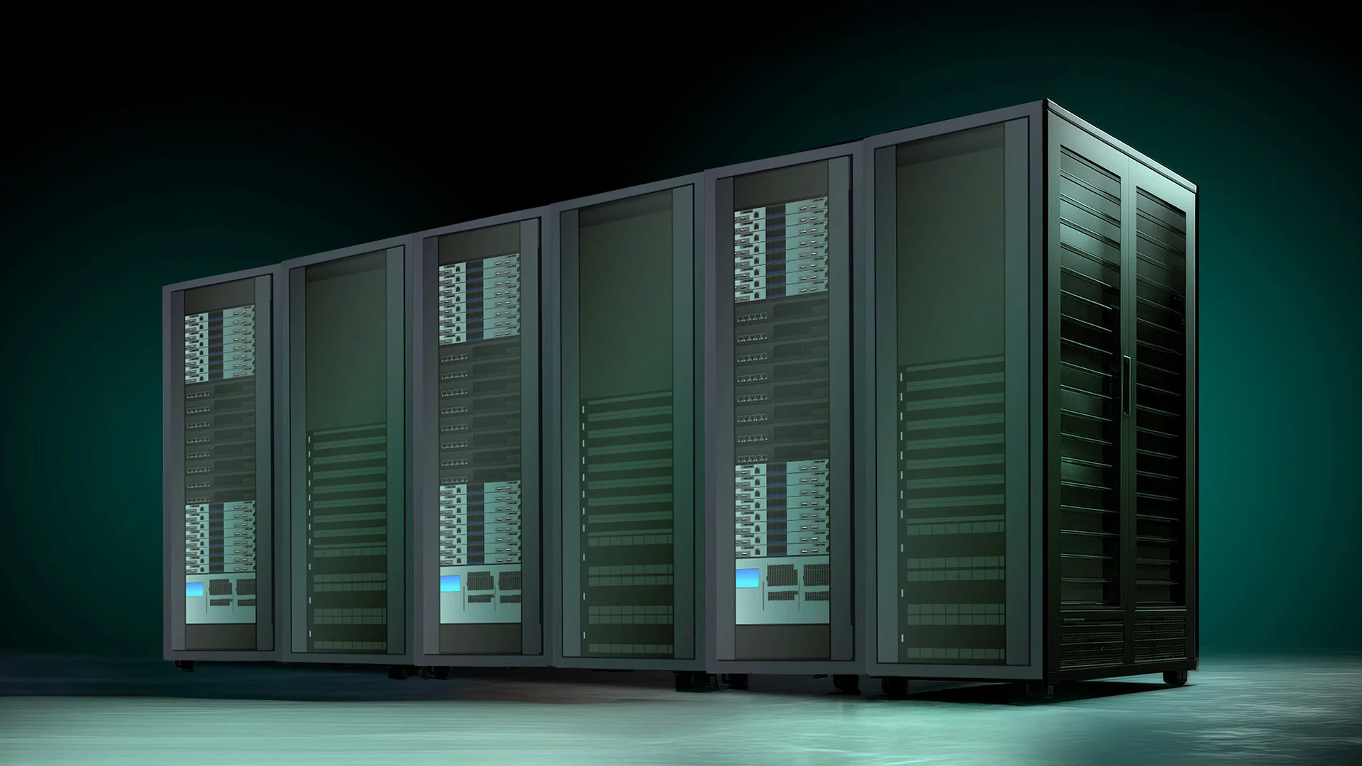
Power delivery in AI data centers is starting to run into a limit that has nothing to do with switching devices or controller bandwidth. The issue is how many times the voltage gets converted before it reaches the silicon. Each stage looks efficient when viewed in isolation, but stack enough of them together and the losses, latency, and thermal overhead begin to accumulate in ways that are difficult to manage at scale.
Texas Instruments is working within that constraint using an 800 VDC power architecture aligned with NVIDIA’s reference design. The structure reduces the traditional multi-stage power tree down to two primary conversion steps between the high-voltage bus and the processor. The 800 V to 6 V and 6 V to sub-1 V stages form a power delivery path used to translate rack-level DC distribution into the voltage domains required by modern AI accelerators. In a typical AI server, power is distributed at high voltage before being stepped down through intermediate rails such as 48 V or 54 V, and then again closer to the load, with each stage balancing efficiency, current handling, and layout constraints.
When Intermediate Rails Start Getting in the Way
Intermediate voltage rails have always been a compromise. They allow power to move through a system without forcing excessive current through copper planes or connectors, but that balance becomes harder to maintain as GPU power demand rises. Lower intermediate voltages mean higher current, and higher current leads to more copper, more heat, and more loss across the distribution network. At some point, the infrastructure carrying the power becomes more difficult to scale than the compute it is supporting, and removing one of those intermediate steps starts to look less like an optimization and more like a necessity.
Collapsing the Power Tree Changes Where Problems Appear
Reducing the number of conversion stages does not eliminate constraints, it simply moves them. What changes is where the stress shows up. Instead of being spread across multiple stages, it concentrates near the load, where current ramps and voltage swings are harder to absorb. When the architecture compresses down to an 800 V to 6 V stage followed by a multiphase conversion to the processor core, the distribution network becomes simpler, but the local power environment becomes more demanding. Current density increases closer to the load, thermal concentration becomes more localized, and transient response tightens because there is less electrical distance to absorb sudden changes in demand.
The Role of High-Density Conversion in This Shift
This only holds together if the conversion stage can run at a density that older designs would struggle to sustain. The 800 V to 6 V stage reduces the need for bulky intermediate infrastructure, but it also places greater pressure on the final stage that drops voltage to the processor core. That stage ends up handling very high current while still trying to keep regulation tight, and once switching behavior, PCB layout, and cooling strategy start interacting at this level, design decisions that were once independent begin to overlap in ways that are not always obvious during initial planning.
AI Power Architecture Is Losing Its Layers
For years, power delivery in data centers followed a layered approach where each stage served a clear purpose and the boundaries between them were well understood. That structure is starting to thin out. Architectures like this one remove stages not because they are inefficient on their own, but because the system as a whole benefits from fewer transitions. It does not simplify the design, it shifts the complexity, and once those intermediate layers begin to disappear, the remaining stages take on more responsibility than they were originally expected to carry.
Learn more and read the original announcement at www.ti.com
Technology Overview
Texas Instruments has introduced an 800 VDC power architecture aligned with NVIDIA’s reference design that reduces AI data center power delivery to two main conversion stages: 800 V to 6 V and 6 V to sub-1 V. This approach minimizes intermediate conversion steps while supporting high-density GPU power requirements.
Frequently Asked Questions
What is TI’s 800 VDC power architecture used for?
It is used in AI data centers to convert high-voltage rack-level DC power into the low-voltage rails required by GPUs and processors.
How many conversion stages are used in this architecture?
The architecture uses two main stages: 800 V to 6 V conversion followed by a multiphase step-down to sub-1 V for the processor core.
You may also like